
Cameras in smartphones will get even better. Sony introduced 2×2 On-Chip Lens technology
According to rumours, such sensors will appear very soon.
Sony has introduced a new technology that will find applications for image sensors for smartphones. If you believe the rumours, the upcoming OpFind X2, to released in the next quarter, will be the first to receive such a sensor camera. It is worth noting that Sony has not yet represented the new technology sensor itself.
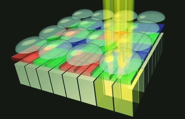
Therefore, this technology called 2×2 on-chip lens (OCL). Sony claims that it has improved its focus speed. Providing higher resolution, higher sensitivity and a wider dynamic range. The image in the image below shows the essence of technology quite simple and nice.
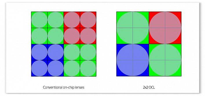
In modern sensors, each pixel gets its own capacitor lunge (lens on-chip). And in new technology, as you can see, four identical neighbouring pixels receive a common lens. Apparently, this technology is only available for use in quad bias sensors. Has prepared.
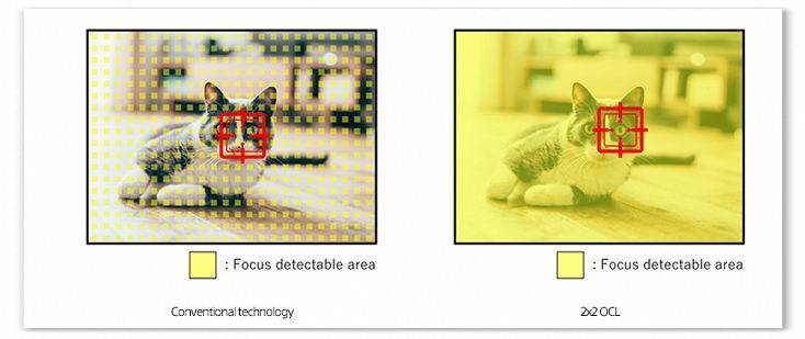
In modern sensors, only a few selected pixels are not used with the imaging functionality to detect the phase difference. And thus the number of pixels is small. In the case of 2×2 on-chip lens (OCL) technology, all pixels can used for these purposes. Which increases focus speed and accuracy, allowing you to focus on smaller objects as well. Gives.
Sony doesn’t talk about the timing of the introduction of the technology in its image sensors.
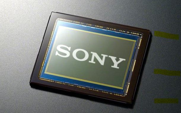
TSMC will release image sensors commissioned by Sony
They will be ready at 40 nm.
According to a source citing a post in the Commercial Times, TSMC has received a Sony order to develop a CMOS type image sensor. They will be manufactured at the Fab 14A factory in Tianan, southern Taiwan, using 40-nanometer process technology.
TSMC has already placed orders for additional process equipment needed to fulfil Sony’s orders. The plant reported to have installed additional 40-nanometer equipment in the second quarter of 2020, and a production schedule scheduled for August next year.
The high and growing demand for image sensors has allowed Sony to consolidate its position in the semiconductor product market and enter into the top ten manufacturers of these products.
Also Read: